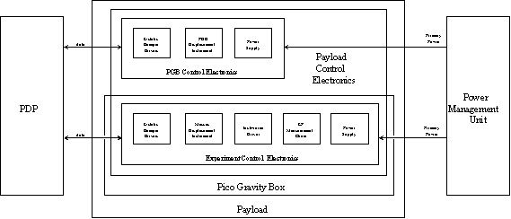
The GG Payload Electronics is composed by two major sub-systems: The Payload Control Electronics (PCE) and the Payload Data Processor (PDP). The former is in charge of performing active damping to the PGB and test masses and performing data acquisition from the sensors, while the latter does processing of data received from the Payload Control Electronics, TLC/TLM management, S/C interface and FEEP thrusters actuation for drag free control.
4.3.1 Payload Control Electronics Architecture
The purpose of the GG Payload Control Electronics is to perform the EP violation measurement, detected as a differential displacement between the two test masses, and to provide active damping against potentially unstable spurious motion (whirling) of the three suspended bodies (PGB and test masses). The active damping will be performed via a closed loop system based on capacitance sensors for positions determination of the body to be damped and electrostatic active dampers as actuators. The following paragraph provides an overview of the P/L Control Electronics sub-system architecture, highlighting the identified critical areas.
Fig. 4.10 shows the GG P/L Control Electronics block diagram; two separate sub-systems can be identified:
Figure 4.10 GG Payload Electronics
This architecture was identified with the specific aim to minimize the number of wires crossing the PGB springs; using a serial interface (RS-422 or similar) the number of the wires can be reduced to 6 (3 through each PGB spring): power supply (2), RX data (2) and TX data (2).
For further wires reduction, other solutions were investigated (power supply through the springs but data modulated on an RF carrier; battery located inside the PGB, charged through a magnetic coupling and data transferred across an optical interface) but they were discarded due to the serious electrical and/or mechanical drawbacks.
Pgb Control Electronics. The overall sub-system is represented in Fig. 4.11; the PGB displacements along the X and Y axis are detected by the PGB Control Electronics by measuring the capacitance variation between pairs of plates around the PGB. Whirling motions are detected by comparing the upper and lower capacitance plates ‘belts’. On the same principle, the displacements along the Z axis are detected by the capacitance plates located on the PGB top and bottom.
In the proposed architecture, the same capacitance plates are used as Sensors and as Active Dampers. An alternative way foresees separate sensor/transducer plates, in each group of four capacitors, two used as sensors and the other two as actuators.
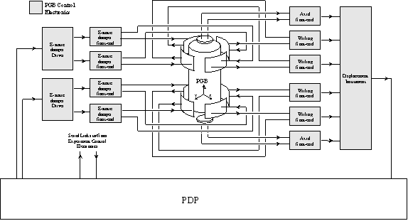
Figure 4.11 PGB Control Electronics
Whirling and Axial Displacement measuring Instrument: this instrument must determine the PGB displacements along the three axes; starting from the variation of the capacitance plates value, it must generate a numerical value proportional to the PGB displacement. These values are transferred to the PDP for further processing (Active Dampers output value calculation and telemetry to ground).
The capacitance variation allows to achieve the measurement resolution (
0.01 µm) imposed to the acquisition system; the GG instrument design will be based on well established guidelines and techniques used in laboratory instruments that provide, without any particular problem, the required accuracy.Electrostatic Damper Driver: starting from the PGB position, determined by the dedicated instrument, the PDP will evaluate the magnitude of the force that must be applied to the PGB through the Active Electrostatic Dampers.
This parameter will be transferred (through a serial line) to the Electrostatic Drivers that generate the voltage applied to the capacitance plates.
It will be possible to modulate the force applied to the PGB by means of a programmable voltage generator able to generate up to
1 kV with 255 steps resolution.Experiment Control Electronics This sub-system will measure the differential displacements and provide active damping to the test masses. The operating principle applied for the Test Masses active damping is similar to the one used for the PGB and previously explained.
The scientific chain will include a displacement sensor based on a capacitance detector much more sensitive than that used for the active damping loops. Two identical scientific chains are foreseen on orthogonal axes.
The architecture of the the Experiment Control Electronics, whose architecture is represented in Fig. 4.12. Note that as a baseline approach the same capacitance plates are used as Whirling Sensors and Active Dampers, or as two different pairs in each group of four capacitances.
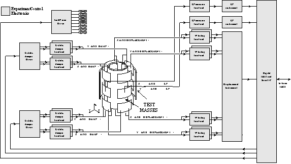
Figure 4.12 Experiment Control Electronics
Whirl Sensing: on the same principle as the PGB, the position of each Test Mass with respect to the PGB will be monitored through eight capacitance plates located on the top and bottom of the Test Mass itself, measuring its displacements along the
X and Y axis.The capacitance variation provided by the capacitance
plates (C » 3 pF, D C » 3× 10⁻³ pF @ 1 µm) is of the same order of magnitude as that for the PGB; as baseline an instrument identical to the one used to determine the S/C-PGB displacement will be used for this purpose.Electro-Static Damper Driver: the force that is to be applied to the Test Masses will be computed by the PDP on the basis of the measured positions and then translated into a voltage to be supplied to the capacitance plates by these drivers.
In order to minimize noise interference between the Active Dampers and the Scientific Measurement Chain, an operating voltage lower
(£ 300 V) than the one used externally to the PGB has been selected. Like the external damper drivers, these too will be 255-steps programmable devices.Inchworm Driver: used to adjust the capacitance plates position. The design of these drivers will be based on well established techniques used in Scanning Tunneling Microscopy (STM) and Atomic Force Microscopy (AFM) applications.
A commercial inchworm controller can easily achieve
10 Å resolution while a high-performance inchworm controller can achieve a resolution of 0,6 Å (Chen X. et al.,1992).In the proposed architecture, one driver (or two if required for symmetrical operation) switched between the inchworms is foreseen.
EP Measurement Chain: this instrument must measure the differential displacement between the Test Masses due to the EP violation, which is the purpose of the GG mission.
This measurement chain must possess extremely high sensitivity as the expected differential displacement of the two test masses related to an EP violation of one part on
1017 is about 0.58 pm (pico-meters). The above sensitivity requirement is extremely challenging, comparable or beyond what is achieved by measurement techniques such as laser interferometry. A well established laboratory technique for non-cryogenic subnanometric displacement measurement is based on the use of balanced capacitive bridges (Jones R. et al., 1973); the same approach has then been chosen the EP measurement in the GG mission.A block diagram of the foreseen EP detector arrangement is shown in Fig. 4.13.
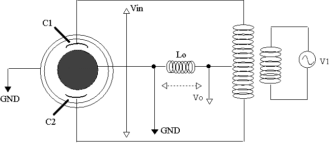
Figure 4.13 EP Measurement Chain with an LC bridge. Another option (capacity bridge) is shown on Fig. 3.10 and is currently mounted and in use in the GGG prototype.
The two test masses
A and B are assumed to be at ground potential, the plates in between are the detecting elements. A high stability ratio-transformer is used to supply the detecting plates, also forming a moderately high Q resonant circuit.The
V1 generator will be the output of a local oscillator running at the bridge resonating frequency F0. The value of this resonating frequency F0 will be driven by a trade-off between various constraints: higher frequencies are preferred in order to reduce the 1/f noise contribution and with the aim of having smaller sizes coils, while lower frequencies are preferred in order to avoid speed constraints on the electronic components. Suitable values of F0 seem to be between 10 kHz and 1 MHz.Making some simplifying assumption it can be shown that the output signal
V0 from the above circuit is given by the following expression:![]() (4.1)
(4.1)
where
C1o and C2o are the "nominal" values of C1 and C2 when the system is perfectly centered (no differential displacement). The V0 signal will be sinusoidal with the same frequency as the driving signal V1, its amplitude will be modulated by the (C1-C2) term.If the measuring plates are well placed just in the middle of the gap between the test masses with an accuracy of the order of some
1.9 m m (see Sec. 2.2.1) (using the inchworms) the (C1-C2) term is dominated by the differential displacement between the plates, as is the effect expected from an EP violation. In such a situation the EP-related modulating signal (C1-C2) as function of time is a periodic signal at the same frequency as the satellite spin (2 Hz) modulating the Vin carrier of frequency F0.With the present mechanical design data the expected differential displacement between the masses is estimated to produce a voltage V0 with an amplitude of the order of
2nV. The EP violation signal is then obtained as a sine wave carrier with frequency F0, amplitude-modulated by a 2 Hz sine wave with 2 nV amplitude. The detection and measurement of such low-level signals demands (apart from a carefully design of the low noise preamplifier) the use of a synchronous detection technique, that in this application is simplified by the fact that we can use the local oscillator itself as reference signal. Fig. 4.14 shows a high-level block diagram of the foreseen electronic chain.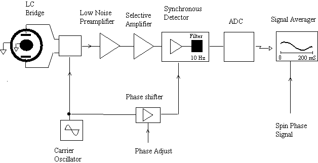
Figure 4.14 High Level Block Diagram for the EP Electronic Chain
In the following we give some details of the various stages of the chain, highlighting the most important features.
The EP detector is constituted by the LC bridge described in the previous paragraph. Particular care should be devoted to the physical connection between the detecting plates and the other components of the bridge as these connection will introduce a certain amount of disturbing effects such as non-stable stray capacitance and noise pick-up. A rigid coaxial connection (like an RF-plumbing) may be adopted to limit above disturbances. The implementation of above connection should also be very symmetric in order to avoid the introduction of unwanted differential "offset" signal. An "ovenised" approach could also be followed so as to operate the bridge in a highly stable thermal environment in order to stabilize all parasitic influences.
As shown in the above diagram, the first stage after the LC bridge is a "low noise amplifier" whose purpose is to provide an impedance and signal level matching between the detector (LC bridge) and the following stages. The design of this amplifier will use state-of-the-art low noise design, a goal of
10-7 pF/Ö Hz equivalent input noise spectral density has been reached in recent work and will constitute the design starting point.The stage following the preamplifier will be a selective amplifier having high gain (
120-140 dB) and a very narrow bandwidth (some hundreds of Hz) centered around the carrier frequency F0 in order to limit noise components amplifications. This stage will be an AC-coupled multistage in order to avoid offset amplification along the chain. The output of the selective amplifier will be put at the input of a synchronous detector locked on a phase-shifted replica of the local carrier F0.The synchronous detection technique is commonly used when a periodic signal of known shape is to be extracted from noise, the output of this stage will be a low frequency signal whose amplitude follows that of the amplitude-modulated carrier i.e. proportional to the differential mass displacement in the detector. The phase shift will be adjustable on board in order to maximize the circuit sensitivity. The
2-phase synchronous demodulation circuits built and used for this purpose in the GGG prototype are shown in Fig. 3.11.The signal at the synchronous detector output is then A/D (analog-to-digital)converted with 16 bit resolution for serial transmission outside the PGB for further processing. The circuit built for this purpose and used in the GGG prototype is shown in Fig. 3.12. The foreseen conversion sample rate is
20 Hz. The last stage of the EP detection chain could be a "signal averager" (maybe S/W implemented inside the PDP). The purpose of this stage is to average the EP data samples synchronously with the spin phase signal (from attitude sensors) in order to extract the actual EP violation signal from possible other effects leading to differential test mass displacement. The operation of the signal averager, synchronous to the spin phase, can be viewed also as a second synchronous detector locked at the spin frequency and indeed could also be realized by H/W in that way.The gain of the overall detecting chain will be set in order to have a full-scale of ±
50 % around the ‘centre’ position. Proper signal for upper and lower out-of-scale will be generated in order to allow the initial centering of the measuring plates by means of the inchworms. A certain amount of on board gain setting could also be provided.4.3.2 Payload Data Processor Architecture
The Payload Data Processor (PDP) will be an electronic unit in charge of performing all the tasks related to payload data processing, payload management and Drag Free Control (DFC). Its main tasks will therefore be:
The PDP computer will be based on a proven design and flight qualified hardware. The proposed processor is the TSC21020, a powerful
32 bit DSP functionally and electrically equivalent to the well known Analog Devices ADSP21020, but realised in radiation tolerant technology and fully qualified for space applications by Temic. The processor has been selected mainly for the following characteristics:Although DSP processors like this are targeted to computationally intensive applications, the TSC21020 performs very well also in data handling tasks. Its choice is therefore adequate for the PDP computer where both the two types of tasks are present, giving a quite large safety margin in the available processing power. A general block diagram of the proposed PDP unit is shown in Fig. 4.15.
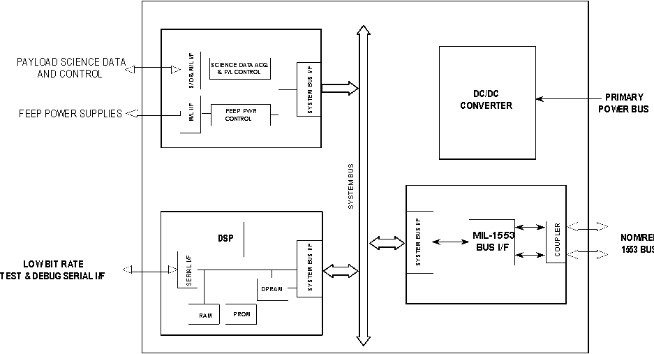
Figure 4.15 Payload Data Processor block diagram
A brief description of the overall architecture of the PDP and of the various blocks is given below.
Architecture. The PDP electronic unit is composed by four boards: three digital boards for data processing and one DC/DC converter for units power supply. The digital boards are interconnected by a
16 bit parallel system bus (the Laben standard SBUS90), which allows to exchange data at high speed among master and slave boards.Microcomputer Board. This board performs the tasks of science data processing, P/L control, DFC algorithm, FEEP power supplies control and TM/TC packets handling. A block diagram is shown in Fig. 4.16.
The board is based on the Temic 32 bit DSP TSC21020. The processor is equipped with 8 Bytes of PROM memory containing the bootstrap program and the emergency/maintenance code,
512 Bytes of non volatile EEPROM memory storing the application SW, 128 Kwords (48 bit per word) of static RAM for program memory and, optionally, up to 256 Kwords (32 bit per word) of static RAM for data memory. At power-on, the bootstrap program stored in PROM copies the application program from EEPROM to program RAM, from where it is actually executed. The execution from program RAM instead of EEPROM allows a faster execution and the possibility of temporary patches of the code. Permanent patches/upgrades of the application code are in any case possible, even in flight, by rewriting the EEPROM content by maintenance code residing in PROM.All the RAM can be optionally protected from soft errors induced by heavy ions radiation which are normally present in space, by means of an error detection and correction circuit (EDAC) able to automatically correct any single bit error in each RAM word and detect double bit errors without CPU intervention. If a periodic scrubbing of the RAM content (i.e. reading and rewriting each word) is done, the probability of erroneous reading of the RAM becomes practically zero even using memory devices less resistant to radiation but cheaper. A trade off is generally made depending on mission requirements and orbit characteristics, taking also in account that the EDAC circuits require additional memory and decrease the CPU speed.
The board includes, in addition to the peripherals already included in the DSP device (timer, interrupt controller, etc.), a serial asynchronous full-duplex channel with RS422 interface, which can be used for testing and debugging as well as for application purposes. It also includes an interface to the system bus with master and slave capabilities, which allows the CPU to communicate with the other boards of the unit.
Additional peripherals or memory can be added directly to the microcomputer board by means of mezzanine boards. Program test and debugging are possible via the JTAG port of the DSP and the access to the program memory bus available on a specific test connector.
MIL-1553 board. The MIL-1553 board allows to interface the PDP unit to the spacecraft data bus which is a MIL-STD-1553 bus. Core of the board is a space qualified hybrid device which implements the functions of Remote Terminal (RT) and Bus Controller (BC) interfacing a generic microcomputer system on one side and a pair of nominal/redundant MIL-1553 busses on the other side. The board also includes an interface to the units system bus by which the DSP can communicate with the hybrid to send to, and receive from, the spacecraft TM/TC packets over the 1553 bus.

Figure 4.16 Microcomputer board block diagram
FEEP and Payload Interface Board. This board interfaces the payload in order to control the payload instruments and to receive scientific data. It also interfaces the various power supplies of the FEEP thrusters to control the thrust according to the Drag Free Control algorithm results.
Both interfaces are of digital type, in the style of the standard Memory Load (ML) / Serial Digital (SD) serial channels. These interfaces are accessible by the microcomputer board via the system bus.
The payload interface is composed of one outgoing ML channel for payload commanding and one incoming SD channel for science and housekeeping data acquisition.
The FEEP interface is composed by one ML channel for Emitter HV power supply control and 6 ML channels for Accelerator + Neutralizer power supplies control (one for each thruster).
This is the baseline configuration. Additional simple interfaces (e.g. thermistors or analog monitors acquisition) can be easily added in case of need.
![]()
![]()